


- Thermal Diffusion of Fullerene Acceptors Changes Morphology of Planar Heterojunctions
Yuri Kim and Tack Ho Lee†

Graduate Department of Chemical Materials, Institute for Plastic Information and Energy Materials, Sustainable Utilization of Photovoltaic Energy Research Center, Pusan National University, Busan 46241, Korea
- 열 어닐링에 의한 풀러렌 유도체 확산에 따른평면 이종접합의 모폴로지 변화
김유리 · 이택호†
부산대학교 화학소재학과
Reproduction, stored in a retrieval system, or transmitted in any form of any part of this publication is permitted only by written permission from the Polymer Society of Korea.
While bulk heterojunction (BHJ) organic solar cells have demonstrated high performance, they face stability challenges. This study introduces an approach to control vertical phase separation of an almost complete bilayer structure by thermal annealing. Planar heterojunction (PHJ) organic solar cells are fabricated using PC71BM/PTB7-Th bilayers through spin coating and film transfer. This method minimizes interlayer mixing and allows control of mixed regions via annealing time. PC71BM diffusion created additional percolation pathways, affecting device characteristics. PHJ devices maintain 65% of their initial efficiency after 8 h of thermal stability testing at 100 ℃, while BHJ devices degrade to a quarter of the initial efficiency. This study demonstrates that the formation of additional percolation pathways in PHJ can potentially improve both the performance and stability of organic solar cells.
벌크 이종접합(BHJ) 유기 태양전지는 높은 성능을 보이지만 안정성 문제에 직면해 있다. 본 연구는 거의 완전한 이중층 구조와 열 어닐링을 사용하여 수직 모폴로지를 제어하는 새로운 접근법을 소개한다. 스핀 코팅 및 필름 전사 방법을 통해 풀러렌 유도체인 PC71BM과 고분자 도너인 PTB7-Th 이중층 평면 이종접합(PHJ) 유기 태양전지를 제작했다. 이 방법은 층간 혼합을 최소화하고 어닐링 시간을 통해 혼합 영역을 제어할 수 있게 한다. PC71BM 확산은 추가적인 투과 경로를 생성하여 소자 특성에 영향을 주었다. 100 ℃에서 8시간 동안 진행된 열 안정성 테스트에서 PHJ 소자는 초기 효율의 65%를 유지한 반면, BHJ 소자는 초기 효율의 4분의 1수준으로 저하되었다. 이 연구는 PHJ에서 추가적인 투과 경로 형성이 유기 태양전지의 성능과 안정성을 동시에 개선할 수 있는 잠재력을 가지고 있음을 보여준다.
This study introduces an approach to control vertical phase separation in planar heterojunction (PHJ) organic solar cells through thermal annealing. PHJ devices demonstrate superior efficiency retention compared to bulk heterojunction (BHJ) devices after a thermal stability test at 100 ℃.
Keywords: organic solar cells, planar heterojunctions, fullerene acceptors, molecular diffusion.
This work was supported by a 2-Year Research Grant of Pusan National University
The authors declare that there is no conflict of interest.
Information is available regarding the contact angle images and AFM images. The materials are available via the Internet at http://journal.polymer-korea.or.kr.
PK_2025_049_04_417_Supporting_Information.pdf (750 kb)
Supplementary Information
Organic solar cells (OSCs) have recently garnered significant attention due to their potential advantages, including lightweight, flexibility, controllable transparency, and solution processability for large-area fabrication.1-3
The bulk heterojunction (BHJ) has been widely adopted as the primary photoactive layer structure in OSCs. This is due to its ability to enhance exciton dissociation by providing sufficient donor-acceptor interfaces through the well-mixed donor-acceptor phases. Recently, with the development of photoactive layer materials, both binary and ternary BHJ OSCs have achieved efficiencies over 19%.1,4
However, the randomly mixed donor-acceptor phases of the BHJs have a complex structure, which increases the bimolecular recombination during the collection of dissociated charges over time.5
Therefore, it is necessary to explore different methods to control the vertical phase distribution in organic solar cells.
In contrast to BHJ structures, planar heterojunction (PHJ) structures offer advantages in device characteristics. Firstly, the well-defined interfacial structure in the PHJ is expected to positively impact long-term structural stability. While achieving high power conversion efficiency (PCE) is critical, the long-term stability is vital to the commercial success of OSCs. In general, the BHJ is tightly optimized, so its metastable morphology is easily altered by external factors such as temperature, light, and moisture.6
Secondly, after charge separation at the donor/acceptor interface in the PHJ, directional carrier transport can increase the charge carrier lifetime.7
Lastly, the vertical distribution of donors and acceptors in PHJ devices can reduce energy losses associated with charge-transfer states, resulting in higher open-circuit voltage (VOC) and suppression of dark current.8,9
Herein, we compare the thermal stability and the performance between PHJ and BHJ OSCs, as well as PHJ-derived devices with additional percolation pathways. The PHJ OSCs were prepared by the film transfer processes on water to prevent the mixing of donor and acceptor layers, enabling more definitive donor/acceptor interfaces. The film transfer method followed the reported procedure.10
The poly[4,8-bis(5-(2-ethylhexyl)thiophen-2-yl)benzo[1,2-b:4,5-b]dithiophene-co-3-fluorothieno [3,4-b]thiophene-2-carboxylate] (PTB7-Th) films were formed on an aqueous surface and then transferred onto the [6,6]-phenyl-C71-butyric acid methyl ester (PC71BM) film. Thermal annealing process on the PHJs was carried out to control these regions according to the annealing time. The vertical morphology of the PHJ devices (mixing of donor and acceptor) was additionally controlled by exploiting the diffusion properties of the fullerene acceptors in the thermal annealing process.11,12
As the glass transition temperature of the polymer donor PTB7-Th is approximately 129 ℃,13
the annealing temperature was chosen as 100 ℃ to minimize film degradation while creating amorphous regions for PC71BM diffusion. Through this procedure, the BHJ morphology characteristics were partially adopted in the PHJ devices.
When devices had morphologies closer to the PHJ, they exhibited higher VOC and lower dark current. In addition, thermal stability tests conducted at 100 ℃ for 4 h in an Ar atmosphere show that PHJ and PHJ-derived devices demonstrate better thermal stabilities compared to the BHJ devices. However, due to the short exciton diffusion length of fullerenes, there were limitations in achieving sufficient film thickness for light absorption, which constrained improvements in the short-circuit current density (JSC) and fill factor (FF) of PHJ-based devices.8,14
Materials. Zinc acetate dihydrate (99.9%), 2-methoxyethanol (99.8%), ethanolamine (99.5%), chlorobenzene, and chloroform used in this study were purchased from Sigma Aldrich (Korea). PTB7-Th was obtained from Solarmer (China), and PC71BM was procured from OSM (Korea). All solvents used in the preparation of solutions were of anhydrous grade.
The structure and energy band alignment of the materials used in the photoactive layer are shown in Figures 1(a) and 1(b). As reported in previous studies, the PTB7-Th film exhibits broad light absorption in the range of 300-800 nm, and the PC71BM film has the complementary light absorption (Figure 1(c)).15
Device Fabrication. The OSCs were fabricated in an inverted structure, consisting of ITO/ZnO/active layer/MoO3/Ag. The ITO-coated glass substrates were cleaned in deionized water, acetone, and isopropanol by ultrasonication. The ZnO layer was spin-coated on the ITO substrate at 3000 rpm for 40 sec using a sol-gel method. The ZnO precursor solution was prepared by dissolving zinc acetate dihydrate in 2-methoxyethanol (100 mg mL-1), with the addition of ethanolamine. For the fabrication of PHJ films, PC71BM films were first spin-coated on the ZnO layer using a 12 mg mL-1 solution of PC71BM in chloroform, followed by thermal annealing at 80 ℃ for 1 min in an Ar-filled glovebox to remove residual solvent. PTB7-Th films (20 nm) were transferred onto the PC71BM films using a water transfer method, where a 10 mg mL-1 solution of PTB7-Th in chlorobenzene with 1 vol% 1,8-diiodooctane was dropped onto deionized water in a petri dish, then the formed polymer layer was transferred after the solvent evaporated. The films were thermally annealed at 100 ℃ for 10, 40, and 80 min in the Ar-filled glovebox. The overall thickness of the PC71BM/PTB7-Th PHJ films were 90 nm, and they were compared with 150 nm thick BHJ films. The BHJ films were prepared onto the ZnO layer by spin-coating a mixture of PTB7-Th:PC71BM (1:1.5 weight ratio, total 27 mg mL-1) dissolved in chlorobenzene:1,8-diiodooctane (97:3 volume ratio). The BHJ films were dried in a vacuum chamber for 6 h to remove residual solvent. Subsequently, MoO3/Ag (8/100 nm) was thermally evaporated under a pressure of less than 5×10⁻⁶ Torr. The active area of the device was 0.08 cm2.
Characterization. J–V curves were measured using Oriel Sol3A Class AAA solar simulator (model 940443A) from Newport (USA) calibrated with a standard photovoltaic cell equipped with a KG5 filter, under AM1.5G (100 mW cm-2) illumination with a source measure unit (Keithley 2400, 2635B). External quantum efficiency (EQE) spectra were measured by using an Oriel® IQE-200TM system from Newport (USA) with a 250 W quartz tungsten halogen lamp as the light source, a monochromator, an optical chopper, a lock-in amplifier, and a calibrated silicon photodetector. The thickness of each film was measured by using a KLA Tencor Alpha-step IQ surface profilometer from KLA Tencor (USA). Tapping mode atomic force microscopy (AFM) images were obtained by using an AFM5000II from HITACHI (Japan). The scan size of the images was 2 × 2 μm with the scan rate of 0.86 Hz and the resolution of 256 pixels per line. Photoluminescence (PL) spectra of each film was measured by using a f-4500 from HITACHI (Japan). Absorption spectra of each film were obtained by using a cary 5000 UV-Vis-NIR spectrophotometer from Agilent (USA).

|
Figure 1 (a) Molecular structures; (b) energy band diagram of PC71BM and PTB7-Th; (c) normalized absorption spectra of PC71BM and PTB7-Th in film. |
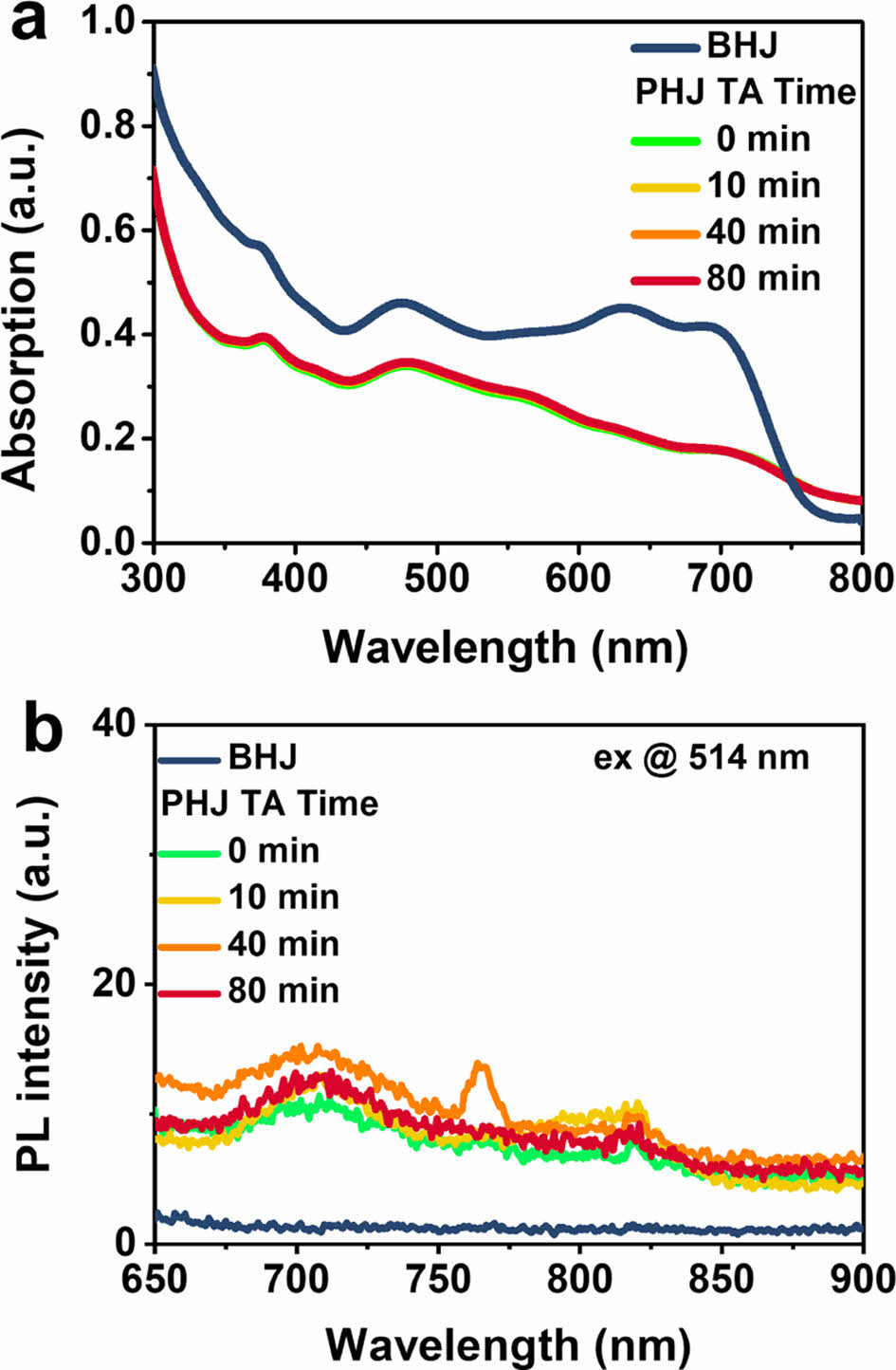
Absorption and Emission Characteristics. The optoelectronic properties of the BHJ and the PHJs were investigated by using absorption and PL measurements. The absorption spectra in Figure 2(a) show that the PHJ films have a relatively lower value than the BHJ film because the PHJ films (90 nm) were thinner than the BHJ film (150 nm). After the PHJ devices were annealed at 100 ℃ in an Ar-filled glove box, the absorption was measured at different annealing time: 10, 40, and 80 min. It was found that there was no change in the absorption spectrum even after 80 min of thermal annealing at 100 ℃.
To investigate exciton separation and charge transfer between PTB7-Th and PC71BM within the film, the degree of PL quenching was examined. The PL emission of PTB7-Th was mainly observed at 760 nm (Figure S1), in agreement with previous reports.15,16
Complete PL quenching was observed in the BHJ film, while photogenerated excitons from PTB7-Th are not completely quenched in the PHJ films with PC71BM regardless of the thermal annealing time. It indicates that the exciton diffusion to the PC71BM/PTB7-Th interface is limited in the PHJ configuration.
Surface Morphology. AFM measurements were conducted to investigate the changes in the film surface morphology by thermal annealing (Figure 3). Surface roughness was measured using the height images from AFM. The root mean square (RMS) of surface roughness for the BHJ was 1.218 nm, while those of the PHJ films were 0.375, 0.469, 0.503, and 0.530 nm for the thermal annealing time of 0, 10, 40, and 80 min, respectively. The BHJ had a rougher surface than the PHJs, and the roughness of the PHJs increased with longer annealing time. Additionally, the range of height distribution became greater with longer annealing time, which could be attributed to the diffusion of PC71BM throughout the entire PTB7-Th film. The BHJ phase image had low contrast indicating that the film was formed with a finely mixed morphology of PTB7-Th and PC71BM. In contrast, the PHJs showed that the contrast of the images increased with longer annealing time, indicating that phase changes could be caused by aggregating PC71BM on the top surface.16 When the thermal annealing time was 0 and 10 min, the contrasts were not prominent, suggesting that the surface was mainly composed of PTB7-Th or that the diffusion of PC71BM had not reached the top surface. However, as the thermal annealing time increased to 80 min, the phase contrasts were gradually increased and distributed on the surface. Therefore, it can be inferred that diffusion of PC71BM occurs as a function of annealing time, and PC71BM aggregation was even observed on top of PTB7-Th film after the thermal annealing of 80 min.
The surface components of the PTB7-Th and PC71BM in the films were analyzed by contact angle measurements. The contact angles of water (polar) and ethylene glycol (nonpolar) on the film surface were measured (Figure S2). The surface energy was calculated from the measured contact angles using previously reported methods (Table 1).2 The surface energy of the pristine PTB7-Th film was 17.69 mN m-1, whereas the pristine PC71BM film showed the higher surface energy of 22.75 mN m-1. The surface energy of the BHJ and PHJ films represents the major components of the top surface. The surface energy of the BHJ film was measured to be 19.28 mN m-1. As a function of the thermal annealing time on the PHJ films, the surface energy was 18.75, 19.18, 19.37, and 19.67 mN m-1 for 0, 10, 40, and 80 min, respectively. It indicates that PC71BM molecules were located on the top surface of the PHJ films after thermal annealing. The ideal vertical D/A phase separation for photovoltaic applications preserves pure donor and acceptor on the top and bottom, respectively, while simultaneously integrating an intermediary mixed region to ensure sufficient D/A interfacial area, as reported in highly efficient layer-by-layer OSCs.17-20 In this work, the thermal molecular diffusion of PC71BM generated additional intermixed regions. However, PC71BM molecules easily penetrated to the top surface due to the thin PTB7-Th layer (20 nm), resulting in undesirable phase separation for good OSCs.
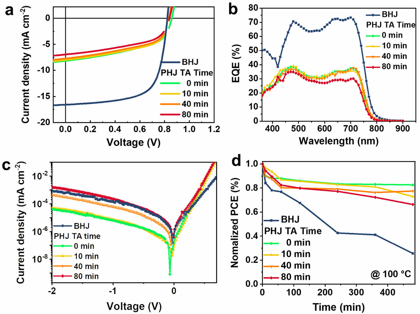
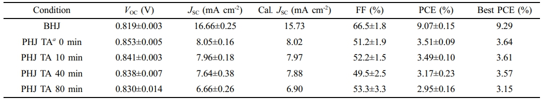
Photovoltaic Properties and Thermal Stability. The performance of photovoltaic cells composed of the BHJ and PHJs is presented in Table 1. For PHJ devices, the JSC was limited to 6-8 mA cm-2, and the external quantum efficiency (EQE) was also limited to below 40%, in agreement with the similar degree of PTB7-Th PL quenching in all PHJ devices (Figure 2(b)). The PC71BM layer of PHJ was 70 nm, and the PTB7-Th layer was 20 nm, which is thinner than the optimal BHJ film thickness of 150 nm. The relatively lower light absorption by the active layer results in lower JSC for the PHJs (see Figure 2(a)). In particular, the PHJ devices thermally annealed at 100 ℃ for 80 min were most affected in the reduction in JSC (from 8.05 to 6.66 mA cm-2) with the PCE decreasing from 3.64% to 3.15% compared to non-annealed devices. The JSC measured from the J-V curve in Figure 4(a) was confirmed to be within the error range of the calculated JSC in Table 2 obtained by integrating the EQE spectrum in Figure 4(b) with the AM 1.5G reference spectrum. The EQE in the 550-800 nm range is mainly attributed to PTB7-Th, while the EQE below 550 nm is primarily due to PC71BM. In Figure 2(a), the absorption spectrum did not change during the 80 min thermal annealing; however, the EQE above 550 nm clearly decreased. This indicates that the PTB7-Th film was not degraded, but the collection of photogenerated charges from PTB7-Th was negatively affected by the 80 min thermal annealing. This can be explained by the diffusion of PC71BM molecules to the top of the PHJ films, as discussed in morphological studies, which could function as recombination sites and contribute to the degradation of overall photovoltaic performance.
In the case of PHJ configuration, the interface between the donor and acceptor is reduced, leading to lower FF compared to the BHJ (Table 2). However, due to the distinct spatial separation of the donor and acceptor, the PHJ devices exhibited a higher VOC than the BHJ device. Additionally, as the thermal annealing time increases, VOC of the PHJ devices slightly decreases. This indicates that the molecular diffusion of PC71BM increases the D/A interfaces by thermal annealing.
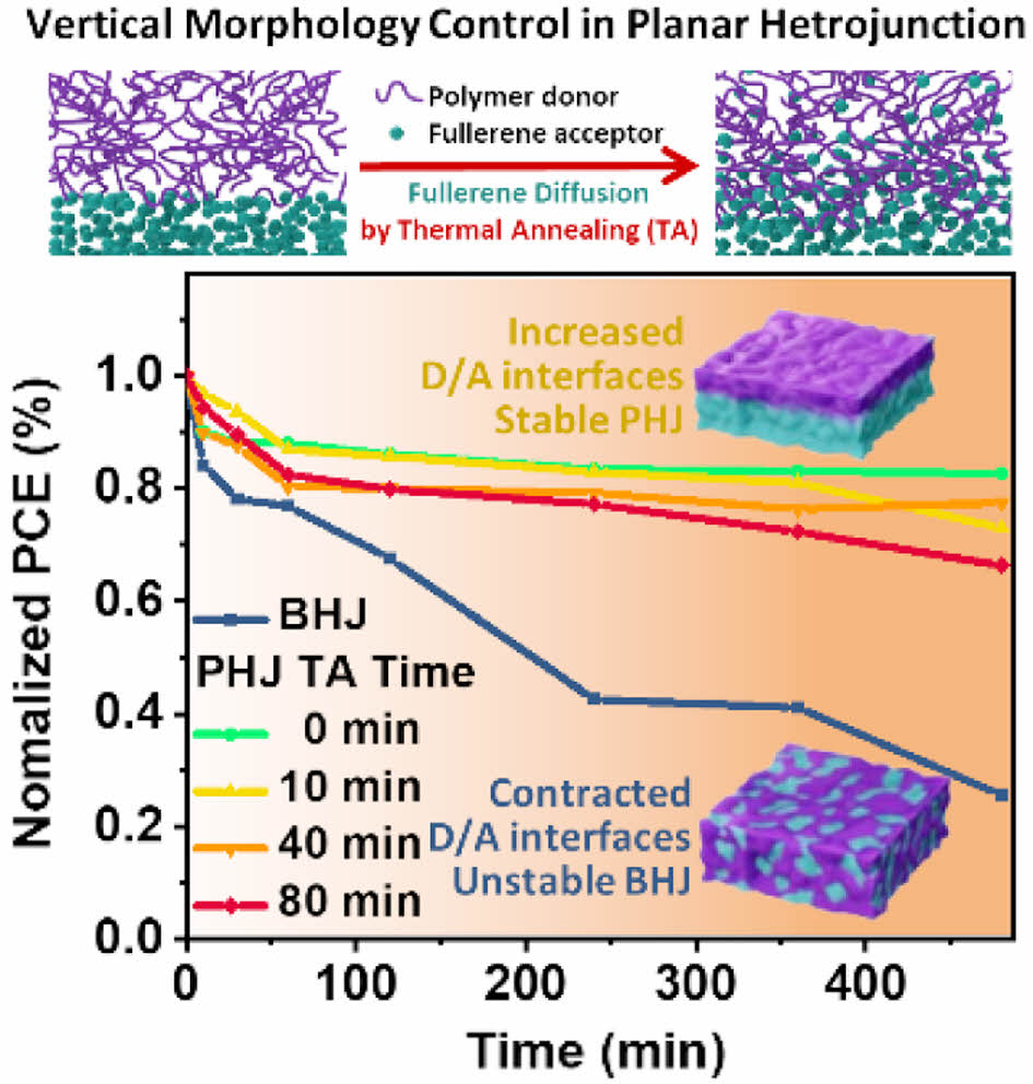
The dark current was also measured to confirm the leakage current under the reverse bias (Figure 4(c)). At -2 V, the current density for the BHJ device was ~10-3 mA cm-2, while the non-annealed PHJ device had 18 times lower dark current. However, as the thermal annealing time of PHJs increased to 10, 40, and 80 min, the dark currents increased and gradually approached that of the BHJ. This indicates that thermal annealing on PHJ devices allows enlarged D/A interfaces in agreement with the VOC of the PHJ devices. To investigate the thermal stability of the devices, thermal stress was applied at 100 ℃ for 8 h. The PHJ devices showed comparatively higher stability than the BHJ devices (Figure 4(d)). While the BHJ devices exhibited a 74% loss of efficiency after 8 h of thermal stress, PHJ devices showed efficiency losses of 17%, 27%, 23% and 34%, respectively. In the case of the BHJ device, its metastable and bi-phase morphology was easily affected by the external thermal stress (Figure S3). In the case of the PHJ devices, on the other hand, the thermal stability of all the PHJ devices was superior to that of the BHJ devices due to the separated donor and acceptor phases (Figure S4). Thermal stability of the PHJ device could be further enhanced by annealing the PTB7-Th film, which can improve molecular packing before being transferred to the PC71BM layer. This confirms that PHJ configuration offers the advantages of lower leakage current and higher thermal stability.
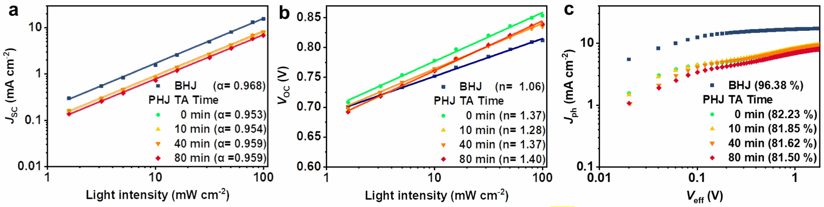
Recombination in Planar Heterojunctions. To investigate the charge recombination losses in the devices, the light intensity dependence of JSC and VOC was measured. Eq. (1) represents the relationship between JSC and light intensity (Plight). When the bimolecular recombination is involved in the device, the α becomes lower than the unity.21

The α for the BHJ was 0.968, which is closer to 1 than the PHJ devices, indicating less bimolecular recombination in the BHJ (Figure 5(a)). The α of the PHJ devices were 0.953, 0.954, 0.959, and 0.959 for the thermal annealing times of 0, 10, 40, and 80 min, respectively, demonstrating almost identical bimolecular recombination properties regardless of the thermal annealing time.
The relationship between VOC and light intensity is given in Eq. (2), where k is the Boltzmann constant, T is the absolute temperature, and q is the elementary charge.22
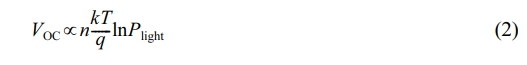
As the value of n is greater than 1, it implies trap-assisted recombination is involved in the devices. The n of the BHJ device was 1.06, and those of the PHJ devices were 1.37, 1.28, 1.37, and 1.40 for the thermal annealing time of 0, 10, 40, and 80 min, respectively (Figure 5(b)). While the non-annealed PHJ device (0 min) had higher VOC than the BHJ device in the whole range of light intensity, the VOC of the annealed PHJ devices decreased and became closer to the VOC of the BHJ device. The primary factor for the observed high VOC in the PHJ devices is the reduced D/A interfacial area and energy losses from charge-transfer states.10,23 The observed decrease in VOC of the annealed PHJ devices correlates with the formation of additional charge transport pathways by the diffusion of PC71BM molecules during the thermal annealing, as discussed in the surface morphology section.
To investigate the exciton dissociation characteristics depending on the structure of active layers, photocurrent density (Jph) versus effective voltage (Veff) curves of the BHJ and PHJ devices are shown in Figure 5(c).24 Jph is the difference between the current density measured under 1 sun illumination (JL) and dark conditions (JD). Veff is calculated as V0-Va, where V0 is the voltage at which JL=JD and Va is the applied bias. Jph* was determined under the short-circuit conditions (Va=0) and Jsat under the saturated state (in this case calculated at Veff=2 V). The exciton dissociation efficiency (ηD) is calculated as Jph*/Jsat. The ηD of the BHJ was 96.38%, while the PHJ devices exhibited around 82%. The higher ηD of the BHJ is attributed to its active layer having a larger interfacial area. PHJ structure has an innate restriction originated from its phase-separated nature, which impedes the ability of efficient exciton dissociation. The comparable exciton dissociation efficiencies were observed in the PHJ devices regardless of the thermal annealing time. This suggests that although the annealed PHJs have larger D/A interfaces, the diffusion of PC71BM molecules to the top surface of PTB7-Th also leads to undesirable charge pathways.
|
Figure 2 (a) Absorption; (b) PL spectra of the BHJ and PHJ films as a function of thermal annealing time (100 ℃). |

|
Figure 3 AFM (a-e) height; (f-j) phase images of (a, f) the BHJ film; the PHJ films for the thermal annealing times of (b, g) 0; (c, h) 10; (d, i) 40; (e, j) 80 min (scale bar: 1 µm). |
|
Figure 4 (a) J-V characteristics under 1 sun illumination; (b) EQE spectra; (c) J-V characteristics in dark; (d) normalized PCE decays as a function of thermal annealing time (at 100 ℃) of the PTB7- Th:PC71BM BHJ device and the PHJ devices. |
|
Figure 5 (a) JSC; (b) VOC dependences on light intensity; (c) Jph vs. Veff curves of the BHJ and PHJ devices as a function of thermal annealing time (100 ℃). |
|
Table 1 Water and Ethylene Glycol (EG) Contact Angle, and the Calculated Surface Energy of Flims |

a TA indicates thermal annealing at 100 ℃ |
|
Table 2 Photovoltaic Parameters of the BHJ and PHJ Devices Fabricated under Various Conditions |
a TA indicates thermal annealing at 100 ℃ |
In this study, the thermal diffusion of PC71BM in the PHJ films with PTB7-Th was investigated by comparison with the control BHJ. Through morphological analysis of the film surface, it was confirmed that thermal annealing induces molecular diffusion and increases D/A interface area in the PHJ devices. However, with longer annealing times, PC71BM molecules diffused further to the top surface of the PHJ structure. These results indicate that the thermal annealing time for ideal vertical phase separation of PHJ devices should be precisely controlled to a certain duration, and prolonged annealing can degrade device performance. The PHJ devices exhibited superior thermal stability, lower leakage current and higher VOC compared to the BHJ device as expected. Our strategy to fabricate ideal vertical phase separation from the PHJ structure by molecular diffusion suggests one of the methods for the high-performing and stable OSCs, which maintain the advantages of the PHJ devices.
- 1. Liu, K.; Jiang, Y.; Ran, G.; Liu, F.; Zhang, W.; Zhu, X. 19.7% Efficiency Binary Organic Solar Cells Achieved by Selective Core Fluorination of Nonfullerene Electron Acceptors Joule 2024, 8, 835-851.
-

- 2. He, X.; Chan, C. C. S.; Zou, X.; Zhang, S.; Fong, P. W. K.; Kim, J.; Li, G.; Hu, X.; Ma, W.; Wong, K. S.; Choy, W. C. H. Modulating the Mixing Gibbs Free Energy to Enhance Solid–Liquid Phase Separation for High-Performance Organic Solar Cells Adv. Energy Mater. 2023, 13, 2203697.
-
- 3. Hu, H.; Ghasemi, M.; Peng, Z.; Zhang, J.; Rech, J. J.; You, W.; Yan, H.; Ade, H. The Role of Demixing and Crystallization Kinetics on the Stability of Non-Fullerene Organic Solar Cells Adv. Mater. 2020, 32, 2005348.
-
- 4. Fu, J.; Yang, Q.; Huang, P.; Chung, S.; Cho, K.; Kan, Z.; Liu, H.; Lu, X.; Lang, Y.; Lai, H.; He, F.; Fong, P. W. K.; Lu, S.; Yang, Y.; Xiao, Z.; Li, G. Rational Molecular and Device Design Enables Organic Solar Cells Approaching 20% Efficiency. Nat. Commun. 2024, 15, 1830.
-
- 5. Kumari, T.; Vyalih, I.; León Luna, M. Á.; Ahmed, H.; Ahmad, M.; Atajanov, R.; Jayaraman, E.; Manikandan, S.; Paci, B.; Di Carlo, A.; Andreasen, J. W.; Turkovic, V.; Madsen, M. Bilayer Layer-by-layer Structures for Enhanced Efficiency and Stability of Organic Photovoltaics Beyond Bulk Heterojunctions. Cell. Rep. Phys. Sci. 2024, 5, 102027.
-
- 6. Zhao, Y.; Wu, Z.; Liu, X.; Zhong, Z.; Zhu, R.; Yu, J. Revealing the Photo-degradation Mechanism of PM6:Y6 Based High-efficiency Organic Solar Cells. J. Mater. Chem. C 2021, 9, 13972-13980.
-
- 7. Liang, Q. B.; Xie, Y.; Wu, H. B. Elucidating the Role of the Heterojunction Interface in the Exciton Harvest and Charge Collection of Organic Solar Cells Through a Planar Heterojunction Structure. J. Mater. Chem. C 2022, 10, 598-606.
-
- 8. Foertig, A.; Wagenpfahl, A.; Gerbich, T.; Cheyns, D.; Dyakonov, V.; Deibel, C. Nongeminate Recombination in Planar and Bulk Heterojunction Organic Solar Cells. Adv. Energy Mater. 2012, 2, 1483-1489.
-
- 9. Kim, T.; Younts, R.; Lee, W.; Lee, S.; Gundogdu, K.; Kim, B. J. Impact of the Photo-induced Degradation of Electron Acceptors on the Photophysics, Charge Transport and Device Performance of All-polymer and Fullerene–polymer Solar Cells. J. Mater. Chem. A 2017, 5, 22170-22179.
-
- 10. Lee, T. H.; Dong, Y.; Pacalaj, R. A.; Park, S. Y.; Xu, W.; Kim, J.-S.; Durrant, J. R. Organic Planar Heterojunction Solar Cells and Photodetectors Tailored to the Exciton Diffusion Length Scale of a Non-Fullerene Acceptor. Adv. Funct. Mater. 2022, 32, 2208001.
-
- 11. Watts, B.; Belcher, W. J.; Thomsen, L.; Ade, H.; Dastoor, P. C. A Quantitative Study of PCBM Diffusion during Annealing of P3HT:PCBM Blend Films. Macromolecules 2009, 42, 8392-8397.
-
- 12. Berriman, G. A.; Holdsworth, J. L.; Zhou, X.; Belcher, W. J.; Dastoor, P. C. Molecular versus crystallite PCBM diffusion in P3HT:PCBM Blends. AIP Adv. 2015, 5, 097220.
-
- 13. Yin, J.; Zhou, W.; Zhang, L.; Xie, Y.; Yu, Z.; Shao, J.; Ma, W.; Zeng, J.; Chen, Y. Improved Glass Transition Temperature towards Thermal Stability via Thiols Solvent Additive versus DIO in Polymer Solar Cells. Macromol. Rapid Commun. 2017, 38, 1700428.
-
- 14. Weng, K.; Ye, L.; Zhu, L.; Xu, J.; Zhou, J.; Feng, X.; Lu, G.; Tan, S.; Liu, F.; Sun, Y. Optimized Active Layer Morphology Toward Efficient and Polymer Batch Insensitive Organic Solar Cells. Nat. Commun. 2020, 11, 2855.
-
- 15. Komilian, S.; Oklobia, O.; Sadat-Shafai, T. Controlling Intercalations of PBDTTT-EFT Side Chain to Initiate Suitable Network for Charge Extraction in PBDTTT-EFT:PC71BM Blended Bulk Heterojunction Solar Cell. Sol. Energy Mater. Sol. Cells 2018, 175, 35-40.
-
- 16. Krishnan Jagadamma, L.; Sajjad, M. T.; Savikhin, V.; Toney, M. F.; Samuel, I. D. W. Correlating Photovoltaic Properties of a PTB7-Th:PC71BM Blend to Photophysics and Microstructure as a Function of Thermal Annealing. J. Mater. Chem. A 2017, 5, 14646-14657.
-
- 17. Cheng, P.; Yan, C.; Wu, Y.; Dai, S.; Ma, W.; Zhan, X. Efficient and Stable Organic Solar Cells via a Sequential Process. J. Mater. Chem. C 2016, 4, 8086-8093.
-
- 18. Mishra, A.; Bhuyan, N. N.; Xu, H.; Sharma, G. D. Advances in Layer-by-layer Processing for Efficient and Reliable Organic Solar Cells. Mater. Adv. 2023, 4, 6031-6063.
-
- 19. Lin, Z.; Du, F.; Wang, H.; Cao, J.; Tang, W. An Unfused-ring Acceptor Enabling ~12% Efficiency for Layer-by-layer Organic Solar Cells. J. Mater. Chem. C 2022, 10, 10511-10518.
-
- 20. Lee, T. H.; Park, S. Y.; Du, X.; Park, S.; Zhang, K.; Li, N.; Cho, S.; Brabec, C. J.; Kim, J. Y. Effects on Photovoltaic Characteristics by Organic Bilayer- and Bulk-Heterojunctions: Energy Losses, Carrier Recombination and Generation ACS Appl. Mater. Interfaces 2020, 12, 55945-55953.
-
- 21. Gayathri, R. D.; Gokulnath, T.; Park, H.-Y.; Kim, J.; Kim, H.; Kim, J.; Kim, B.; Lee, Y.; Yoon, J.; Jin, S.-H. Impact of Aryl End Group Engineering of Donor Polymers on the Morphology and Efficiency of Halogen-Free Solvent-Processed Nonfullerene Organic Solar Cells. ACS Appl. Mater. Interfaces 2022, 14, 10616-10626.
-
- 22. Zhu, L.; Zhang, M.; Zhou, G.; Hao, T.; Xu, J.; Wang, J.; Qiu, C.; Prine, N.; Ali, J.; Feng, W.; Gu, X.; Ma, Z.; Tang, Z.; Zhu, H.; Ying, L.; Zhang, Y.; Liu, F. Efficient Organic Solar Cell with 16.88% Efficiency Enabled by Refined Acceptor Crystallization and Morphology with Improved Charge Transfer and Transport Properties. Adv. Energy Mater. 2020, 10, 1904234.
-
- 23. Vandewal, K.; Widmer, J.; Heumueller, T.; Brabec, C. J.; McGehee, M. D.; Leo, K.; Riede, M.; Salleo, A. Increased Open-Circuit Voltage of Organic Solar Cells by Reduced Donor-Acceptor Interface Area. Adv. Mater. 2014, 26, 3839-3843.
-
- 24. Xu, W.; Zhu, X.; Ma, X.; Zhou, H.; Li, X.; Jeong, S. Y.; Woo, H. Y.; Zhou, Z.; Sun, Q.; Zhang, F. Achieving 15.81% and 15.29% Efficiency of All-polymer Solar Cells Based on Layer-by-layer and Bulk Heterojunction Structures. J. Mater. Chem. A 2022, 10, 13492-13499.
-
- Polymer(Korea) 폴리머
- Frequency : Bimonthly(odd)
ISSN 2234-8077(Online)
Abbr. Polym. Korea - 2025 Impact Factor : 1.0
- Indexed in SCIE
 This Article
-
2025; 49(4): 417-424
Published online Jul 25, 2025
- 10.7317/pk.2025.49.4.417
- Received on Nov 1, 2024
- Revised on Jan 20, 2025
- Accepted on Mar 9, 2025
Services
- Full Text PDF
- Abstract
- ToC
- Acknowledgements
- Conflict of Interest
- Supporting Information
Introduction
Experimental
Results and Discussion
Conclusions
- References
Shared
Correspondence to
- Tack Ho Lee
-
Graduate Department of Chemical Materials, Institute for Plastic Information and Energy Materials, Sustainable Utilization of Photovoltaic Energy Research Center, Pusan National University, Busan 46241, Korea
- E-mail: tackho@pusan.ac.kr
- ORCID:
0000-0003-2201-0165
Hyecheon Building(Room 601), #354, Gangnam-Daero, Gangnam-Gu, Seoul 06242, Korea
TEL : 82-2-568-3860, 561-5203, 569-3860 FAX : 82-2553-6938 E-mail: polymer@polymer.or.kr